IBM UNVEILS SUB 1NM CHIP WITH 100 BILLION TRANSISTORS
A new nanostack architecture doubles transistor density over the 2nm node, adding 10-15 years to the semiconductor roadmap.
by editor4 min readcomments soon
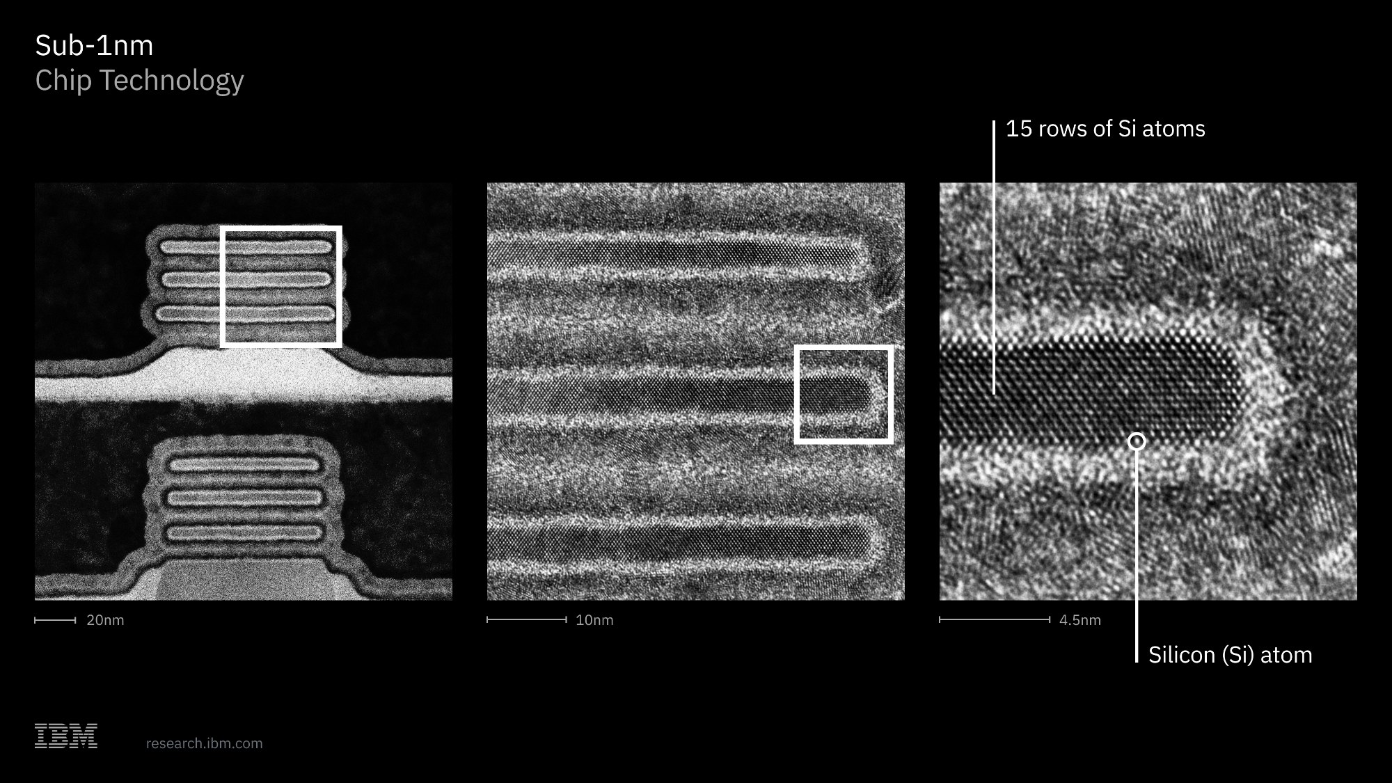
IBM has built the first sub-1 nanometer chip node, a prototype that packs 100 billion transistors onto a chip the size of a fingernail. The node, which IBM calls a nanostack and markets as a 0.7 nanometer process, nearly doubles the transistor density of the company's own 2 nm node from 2021.
The milestone matters because the semiconductor industry has been stuck on a fundamental limitation: the distance between transistors "has been staying at about 40 nanometers for quite a long period of time". IBM's solution is not to shrink the transistors further in the plane, but to stack them vertically. The new architecture stacks two layers of transistors on a single silicon wafer, connected by an innovative dielectric bond. Each transistor uses three nanosheets, each about 15 atoms thick, spaced 9 nanometers apart. The result is a structure that can do up to 50% more work in the same time or consume 70% less energy than IBM's current state-of-the-art chips.



Jay Gambetta, IBM's vice president of quantum and semiconductor technology, called it "It’s a meaningful leap forward.".
HOW THEY GO THERE
IBM's 2 nm node, announced in 2021, already used a nanosheet architecture that marked a significant industry advance. The new node builds on that foundation by stacking the nanosheets vertically across two separate wafers, then bonding them together at low temperature. The challenge was making the second layer of transistors without melting the connections in the first layer, which requires processes below 400 degrees Celsius. IBM figured out how to do it, but the company is not disclosing the exact method.
Outside researchers recognise the difficulty. Qing Cao, a materials scientist at the University of Illinois Urbana-Champaign, described IBM's work as "transformative" because it demonstrates vertical stacking "on a full wafer using a state‑of‑the‑art manufacturing line". Cao's own group has created a method for stacking transistors layer by layer with processes below 200 degrees Celsius, but he notes that IBM's achievement on a full wafer with a commercial manufacturing line is a different league of scale.
THE ROADMAP EXTENSION
Dan Hutcheson, an analyst at TechInsights, said the innovation effectively extends the semiconductor roadmap by a decade or more. "This puts another 10, 15 years on the roadmap." For context, the industry has long predicted the end of Moore's Law as transistor shrinkage becomes physically impossible at atomic scales. By moving into the third dimension, chipmakers can continue scaling performance and density without needing to shrink gate lengths below 1 nm.
The sub-1 nm name is partly marketing. As IBM and others have noted, node names now refer to manufacturing generations rather than precise physical dimensions. But the underlying density gain is real. The new node packs 100 billion transistors on a chip area that previously held roughly 50 billion with the 2 nm process. That doubling density is what enables the 50% or 70% tradeoff between performance and power.
THE COMPETITIVE LANDSCAPE
IBM is a research pioneer but does not manufacture chips at scale. The new node is intended for licensing to fabrication partners such as Intel, Samsung, and TSMC, all of which are working on their own 3D transistor stacking approaches. Imec, the Belgian research institute, has demonstrated a complementary FET architecture that stacks n-type and p-type transistors vertically. AMD uses a stacked cache approach called 3D V-Cache, and there are other logic stacking techniques such as LogicFolding.
IBM's advantage is that its nanostack is demonstrated on a full 300 millimetre wafer using existing manufacturing equipment, which means it could be commercialised faster than more exotic approaches. The question is when and which products will use it. Cao pointed to the need for a killer application: "I’m interested in what’s their killer application." High-performance computing, AI accelerators, and data centre processors are the most likely first users, where the combination of density and energy efficiency directly translates to lower operating costs.
WHAT IT MEANS FOR THE NEXT DECADE
The industry has been stretching planar scaling far beyond what anyone thought possible twenty years ago. Extreme ultraviolet lithography was supposed to be the last tool. Now 3D stacking looks like the next major paradigm. IBM's prototype proves the concept works at wafer scale. The remaining work involves yield, cost, and design tooling. Chip designers need electronic design automation tools that can handle multi-layer transistor layouts, and foundries need to qualify the new process for volume production.



If Hutcheson's estimate of 10 to 15 years of additional roadmap holds, the sub-1 nm node buys time for the industry to figure out the next leap after stacking: optical interconnects, carbon nanotubes, or something else entirely. For now, the immediate takeaway is that the transistor is far from dead. It is just learning to stand up.
what did you make of it?
more from science
science
ARXIVLABS OPENS PREPRINT SERVER FOR COLLABORATIONS
arXiv invites outside developers who share its values of openness, community, excellence, and privacy.
science
NOAA CONFIRMS El NINO IS HERE, COULD BE THE STRONGEST IN 140 YEARS
Oceans have absorbed 23 zettajoules of heat in recent years, the equivalent of 365 million atomic bombs. Now the climate system's best-known disruptor is loading…
science
SCIENTISTS DISCOVER OLDEST WHALE GRAVEYARD
A 2023 expedition found 476 fossilized whales and at least five active whale falls in the Diamantina fracture zone, some dating back 5.3 million years.
science
CORNELL RESEARCHERS RESTORE DISCARDED EV BATTERIES TO 95%
The DEER process soaks electrodes in an electrochemical solution to dissolve the degradation layer, allowing cleaned components to go straight back into new cells without…